- 您现在的位置:买卖IC网 > Sheet目录3879 > DSPIC30F6013T-20I/PF (Microchip Technology)IC DSPIC MCU/DSP 132K 80TQFP
2006
Micr
ochip
T
e
ch
nol
ogy
I
n
c.
DS
70117F
-page
159
dsPIC3
0F601
1/60
12/6013/6
014
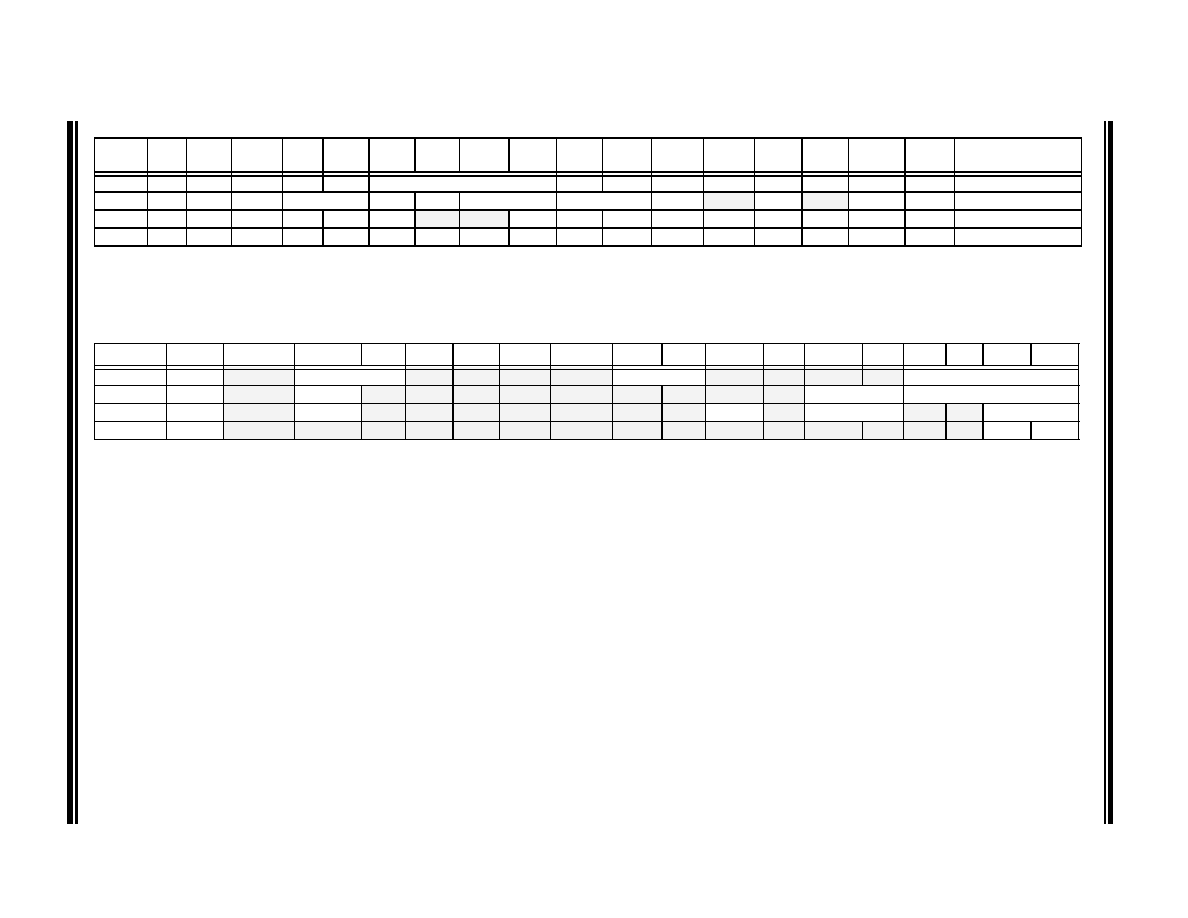
TABLE 20-7:
SYSTEM INTEGRATION REGISTER MAP
TABLE 20-8:
DEVICE CONFIGURATION REGISTER MAP
SFR
Name
Addr.
Bit 15
Bit 14
Bit 13
Bit 12
Bit 11
Bit 10
Bit 9
Bit 8
Bit 7
Bit 6
Bit 5
Bit 4
Bit 3
Bit 2
Bit 1
Bit 0
Reset State
RCON
0740
TRAPR IOPUWR
BGST
LVDEN
LVDL<3:0>
EXTR
SWR
SWDTEN
WDTO
SLEEP
IDLE
BOR
POR
(Note 1)
OSCCON
0742
TUN3
TUN2
COSC<1:0>
TUN1
TUN0
NOSC<1:0>
POST<1:0>
LOCK
—CF
—
LPOSCEN OSWEN
(Note 2)
PMD1
0770
T5MD
T4MD
T3MD
T2MD
T1MD
—
DCIMD
I2CMD
U2MD
U1MD
SPI2MD
SPI1MD
C2MD
C1MD
ADCMD 0000 0000 0000 0000
PMD2
0772
IC8MD
IC7MD
IC6MD
IC5MD
IC4MD
IC3MD
IC2MD
IC1MD
OC8MD OC7MD
OC6MD
OC5MD
OC4MD OC3MD
OC2MD
OC1MD 0000 0000 0000 0000
Note 1:
Reset state depends on type of Reset.
2:
Reset state depends on Configuration bits.
3:
Refer to “dsPIC30F Family Reference Manual” (DS70046) for descriptions of register bit fields.
File Name
Addr.
Bits 23-16
Bit 15
Bit 14
Bit 13
Bit 12
Bit 11
Bit 10
Bit 9
Bit 8
Bit 7
Bit 6
Bit 5
Bit 4
Bit 3
Bit 2
Bit 1
Bit 0
FOSC
F80000
—
FCKSM<1:0>
—
FOS<1:0>
—
—FPR<3:0>
FWDT
F80002
—FWDTEN
—
FWPSA<1:0>
FWPSB<3:0>
FBORPOR
F80004
—
MCLREN
—
—BOREN
—
BORV<1:0>
—
—FPWRT<1:0>
FGS
F8000A
—
GCP
GWRP
Note:
Refer to “dsPIC30F Family Reference Manual” (DS70046) for descriptions of register bit fields.
发布紧急采购,3分钟左右您将得到回复。
相关PDF资料
DSPIC30F6012T-30I/PF
IC DSPIC MCU/DSP 144K 64TQFP
DSPIC30F6012T-20I/PF
IC DSPIC MCU/DSP 144K 64TQFP
DSPIC30F6011T-30I/PF
IC DSPIC MCU/DSP 132K 64TQFP
DSPIC30F6011T-20I/PF
IC DSPIC MCU/DSP 132K 64TQFP
DSPIC30F6010T-30I/PF
IC DSPIC MCU/DSP 144K 80TQFP
DSPIC30F6010T-20I/PF
IC PSPIC MCU/DSP 144K 80TQFP
PIC16C56A-20/P
IC MCU OTP 1KX12 18DIP
PIC16C621A-04I/P
IC MCU OTP 1KX14 COMP 18DIP
相关代理商/技术参数
DSPIC30F6013T-30I/PF
功能描述:数字信号处理器和控制器 - DSP, DSC 30MHz 132KB Flash RoHS:否 制造商:Microchip Technology 核心:dsPIC 数据总线宽度:16 bit 程序存储器大小:16 KB 数据 RAM 大小:2 KB 最大时钟频率:40 MHz 可编程输入/输出端数量:35 定时器数量:3 设备每秒兆指令数:50 MIPs 工作电源电压:3.3 V 最大工作温度:+ 85 C 封装 / 箱体:TQFP-44 安装风格:SMD/SMT
DSPIC30F6014-20E/PF
功能描述:数字信号处理器和控制器 - DSP, DSC 30MHz 132KB Flash RoHS:否 制造商:Microchip Technology 核心:dsPIC 数据总线宽度:16 bit 程序存储器大小:16 KB 数据 RAM 大小:2 KB 最大时钟频率:40 MHz 可编程输入/输出端数量:35 定时器数量:3 设备每秒兆指令数:50 MIPs 工作电源电压:3.3 V 最大工作温度:+ 85 C 封装 / 箱体:TQFP-44 安装风格:SMD/SMT
DSPIC30F6014-20I/P
制造商:Microchip Technology Inc 功能描述:MCU - Rail/Tube
DSPIC30F6014-20I/PF
功能描述:数字信号处理器和控制器 - DSP, DSC 20MHz 144KB Flash RoHS:否 制造商:Microchip Technology 核心:dsPIC 数据总线宽度:16 bit 程序存储器大小:16 KB 数据 RAM 大小:2 KB 最大时钟频率:40 MHz 可编程输入/输出端数量:35 定时器数量:3 设备每秒兆指令数:50 MIPs 工作电源电压:3.3 V 最大工作温度:+ 85 C 封装 / 箱体:TQFP-44 安装风格:SMD/SMT
DSPIC30F6014-20I/PF
制造商:Microchip Technology Inc 功能描述:16BIT 20MIPS DSPIC SMD 30F6014
DSPIC30F6014-30I/PF
功能描述:数字信号处理器和控制器 - DSP, DSC 30MHz 144KB Flash RoHS:否 制造商:Microchip Technology 核心:dsPIC 数据总线宽度:16 bit 程序存储器大小:16 KB 数据 RAM 大小:2 KB 最大时钟频率:40 MHz 可编程输入/输出端数量:35 定时器数量:3 设备每秒兆指令数:50 MIPs 工作电源电压:3.3 V 最大工作温度:+ 85 C 封装 / 箱体:TQFP-44 安装风格:SMD/SMT
DSPIC30F6014-30I/PF
制造商:Microchip Technology Inc 功能描述:16BIT 30MIPS DSPIC SMD 30F6014
dsPIC30F6014A-20E/PF
功能描述:数字信号处理器和控制器 - DSP, DSC 20MIPS 144 KB RoHS:否 制造商:Microchip Technology 核心:dsPIC 数据总线宽度:16 bit 程序存储器大小:16 KB 数据 RAM 大小:2 KB 最大时钟频率:40 MHz 可编程输入/输出端数量:35 定时器数量:3 设备每秒兆指令数:50 MIPs 工作电源电压:3.3 V 最大工作温度:+ 85 C 封装 / 箱体:TQFP-44 安装风格:SMD/SMT